


I. INTRODUCTION
Analog integrated circuits are key hardware components for building new multi-media system applications including internet-of-things (IoT), 5G communication, and self-driving cars [1]. To comply with the emerging trends, new design methodologies for analog integrated circuits that can improve the circuit performance while maintaining good cost and power efficiency are in high demand [2]. Design automation is an ultimate goal for analog integrated circuits, since this can significantly improve the design time and productivity. However, unlike digital integrated circuits, where the design procedure can be fully automated – most of the digital processing algorithms realized using MATLAB codes or hardware description language (HDL) can be directly converted into transistor level circuits within several hours (this is called top-down design), analog circuits have a lot of limitations for design automation. This is mainly due to the non-linear behavior of the transistors that are used as basic elements.
A typical analog circuit design procedure consists of two major steps that are circuit topology selection and transistor biasing. In case of MOS transistors, biasing is setting the transistor size, in other words the aspect ratio (W/L) where W and L are the width and length, and fixing the operating voltages including the gate-to-source voltage VGS and drain-to-source voltage VDS, and the current ID so that the transistor properly operates in the desired operation region [3]. However, due to the non-linear current-voltage (I-V) characteristics of the transistor, transistor biasing heavily rely on the case-by-case experience of the circuit designer and the circuit simulator, which is not very systematic and time consuming.
In this work, in order to overcome the limitations of analog integrated circuit design, in particular reducing the design time, a transistor circuit model based design method that can represent the saturation region operation with linear circuit components is proposed. This is similar to the linear circuit model used for time-mode circuits [4] and image processing circuits [5], however the proposed model is more specialized for MOS transistors. Since the proposed design method can replace the non-linear transistor with a linear circuit model, biasing will be simple and straightforward compared to the conventional design method that deals with the transistor as it is. As a result, the proposed design method can systematically bias the transistors without heavily relying on the designer’s experience and the circuit simulator, which will reduce the design time as well. However, the proposed biasing scheme differs from the well-known gm/ID method which also use charts and tables obtained from pre-simulated transistor data, since the main objective of gm/ID is to optimize the circuit performance and power consumption instead of biasing the transistor [6]. In order to verify the proposed method, a single-ended folded cascade amplifier will be used as a biasing example, where the transistor sizes are set so that the desired operating point is achieved without using the circuit simulator.
II. AUTOMATED BIASING SCHEME
This section will describe the automated transistor biasing method based on linearized transistor circuit model, where an actual amplifier circuit will be used as an example to verify the effectiveness of the proposed biasing scheme.
Fig. 1 shows the single-ended folded cascade amplifier that will be used as the biasing example. This amplifier circuit is widely used in a variety of applications including IoT [7]. Table 1 shows the design constraint where the W of each transistor will be set based on the proposed biasing method such that the transistors operate at the desired DC bias point (VDS and VGS). However, before biasing the transistors, in order to satisfy all the other design constraints, the value of Iss, VB1, VB2, VB3, and RD should be determined.
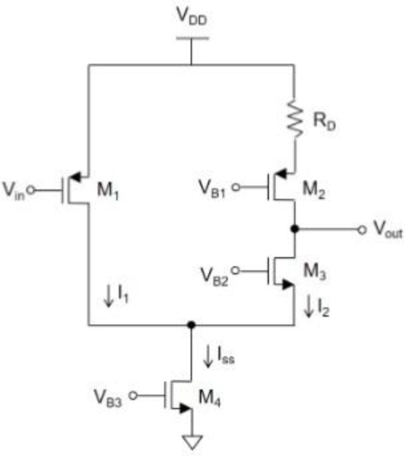
The steering current Iss is bounded by the power consumption PD and the trans-conductance gm which are given as
where Vov1 = VGS1 – VTH and I1 = Iss/2, since I1 = I2 and Iss = I1 + I2. As a result, Iss is set to the smallest possible value 54uA. Next, the input common mode voltage VI,cm and the fixed DC gate bias VB1, VB2, and VB3 are set based on the VDS and VGS requirement of each transistor. VI,cm is set by VDD and VGS1. That is,
VB1 is obtained from the following relationship
Since the source of M4 is tied to GND, VB2 is given as
The gate bias voltages that satisfy the VDS and VGS requirement for each transistor are VI,cm = 2.1V, VB1 = 1.2V, VB2 = 2V, and VB3 = 1V. Also, the value of RD is obtained by
where Vs2 is the source voltage of M2 which is given as
As a result, the value of RD that meets the design constraint is 33.6kΩ.
The proposed transistor circuit model is a linear model that represents the strong inversion saturation region operation of the transistor, since most of the analog circuits are realized based on the saturation region operation. Fig. 2(a) shows the nmos transistor symbol, (b) the proposed circuit model, and (c) the I-V curve that shows the two operation regions. Depending on the value of VDS, the operation region of the transistor can be divided into two regions - linear (VDS < Vov) and saturation (VDS > Vov) where Vov is the boundary voltage that is equivalent to (VGS – VTH) where VTH is the threshold voltage. Although the transistor is a non-linear device, the saturation region can be modeled with simple circuit components such as the current/voltage source and the resistor, since the saturation region current ID has a linear relationship with VDS. Therefore, the key ideal of the proposed transistor circuit model is to divide ID into two components that are the active current IA and the passive current IP, which is represented by the left and right branch in the circuit model. In addition, IA depends on VGS and IP is determined by VDS, Rout, and Vov where Rout is the saturation region output resistance. The expressions for IA and IP of the nmos are given as
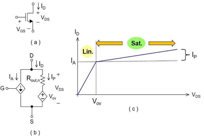
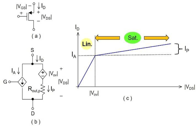
Fig. 3 (a) shows the pmos transistor symbol. (b) the proposed circuit model, and (c) the I-V curve, where the circuit model is similar to the NMOS, except VGS, VDS, Vov, and VTH are negative, and the electron mobility μn will be replaced with hole mobility μp. The expressions for IA and IP of the pmos are given as
Once the VDS, VGS, and ID of the transistors are determined, each transistor in the amplifier circuit will be replaced with the linearized transistor circuit model where W of the transistors are set based on the desired operating point – this is the biasing procedure. Toward this end, we will first find the passive current IP based on eq. (8b) and (9b), and find the active current IA using
However, to avoid heavily relying on the circuit simulator, curve fitted expressions obtained from the pre-simulated data of Rout and IA will be used for finding IP and W of each transistor. The pre-simulation data is obtained using Cadence Spectra mixed signal circuit simulator.
Fig. 4(a) and (b) show Rout vs. ID for the nmos and pmos, where the dots indicate the pre-simulation data and the red line is the curve fitted plot obtained from power fit. The curve fitted expression for the nmos and pmos are given as
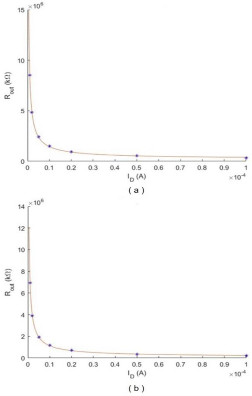
Using the above expressions, Rout at the desired bias current ID can be obtained, where for M1, M2, M3, ID = Iss/2 and for M4, ID = Iss. In addition, Fig. 5(a) and (b) show IA vs. W of the nmos (VGS = 1V) and pmos (|VGS| = 0.9V), where the dots indicate the pre-simulated data and the red line is the curved fitted plot obtained from linear fit. The curve fitted expressions for the nmos and pmos are given as:
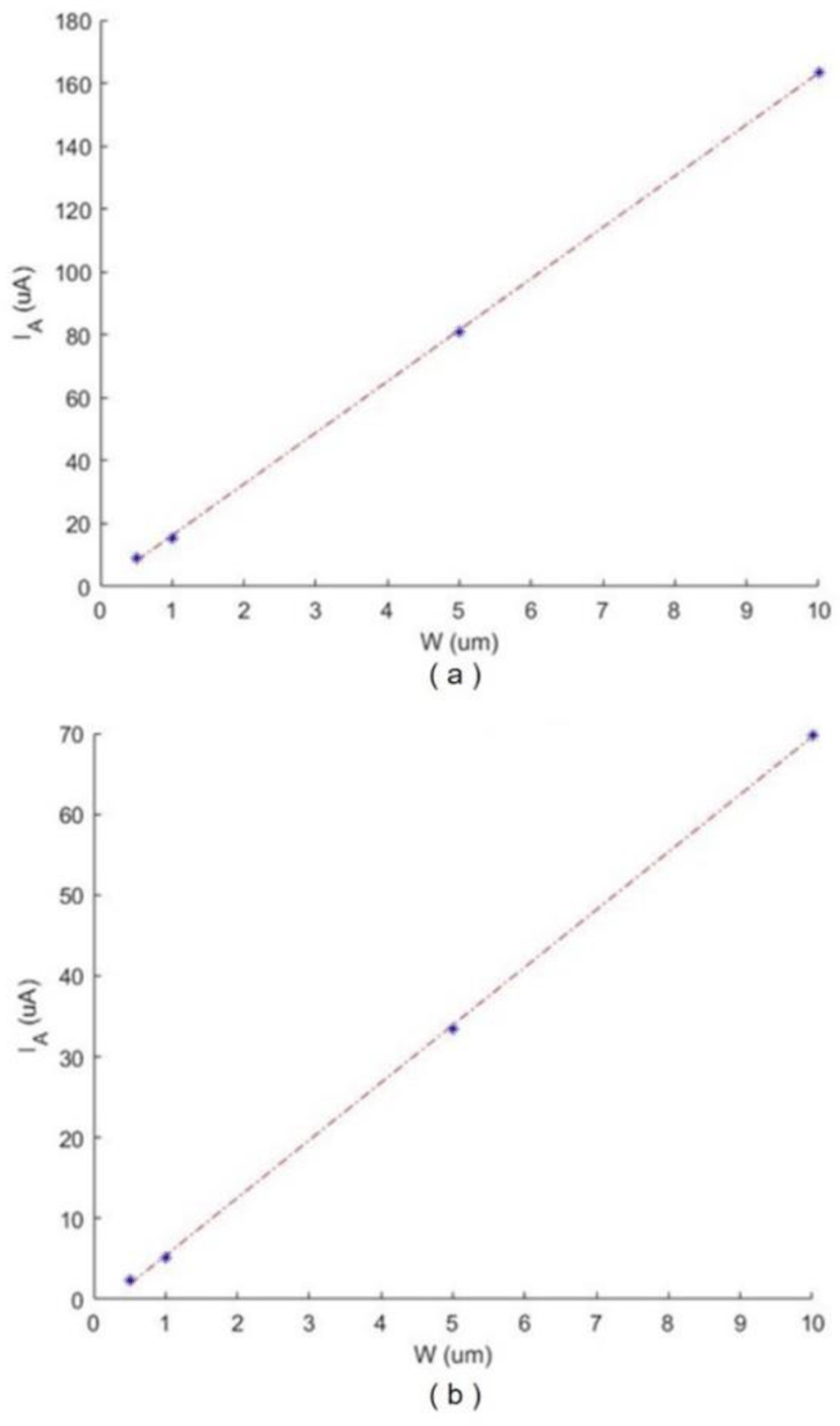
Based on the above expressions, W corresponding to IA can be obtained. This W will enable the transistor to operate at the desired VDS, VGS, and ID. Table 2 shows the Rout, IP, IA, and W of each transistor obtained from the proposed biasing method, where a MATLAB program is used to compute Rout, IP, IA, and W. As shown, the proposed biasing method only use basic pre-simulation data for the nmos and pmos instead of heavily relying on the circuit simulator throughout the entire biasing steps, which can enable a faster design time. Furthermore, to show the effectiveness of the proposed biasing scheme, the same single-ended folded cascode amplifier (Fig. 1) has been biased with the conventional approach (mainly using the circuit simulator), where design (biasing) time of the proposed method showed 10× faster than the conventional method.
| Transistor | Rout (kΩ) | IP (uA) | IA (uA) | W (um) |
|---|---|---|---|---|
| M1 | 548 | 3.37 | 23.63 | 3.61 |
| M2 | 548 | 0.82 | 26.18 | 3.98 |
| M3 | 754 | 0.13 | 26.87 | 1.65 |
| M4 | 516 | 1.16 | 52.84 | 3.30 |
III. CONCLUSION
This work presents an automated transistor biasing scheme for analog integrated circuits based on the linearized transistor circuit model along with the curve fitted expressions obtained from the pre-simulated I-V characteristics of the transistor. As a result, the transistor size that leads to the desired operating point can be easily determined without heavily relying on the circuit sim-ulator, which leads to significant design time reduction. The proposed method is applied to an actual amplifier circuit where the design time based on the proposed biasing method showed 10× faster than the conventional design approach using the circuit simulator. As a future work, the proposed method will be applied to biasing different types of amplifiers.