I. INTRODUCTION
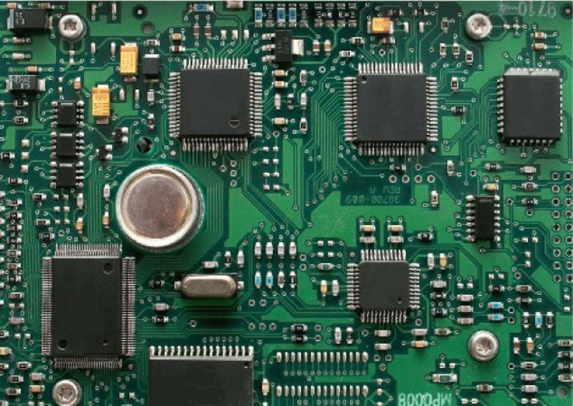
Surface mount technology (SMT) [1] as shown in Fig. 1, is a method in which electronic components are mounted onto the printed circuit board (PCB) [2] to reduce manufacturing costs and make more efficient use of the PCB space. Surface mount devices (SMD) [3] are electronic components used within the surface mount assembly process and it is possible recently to build highly complex electronic circuits into smaller and smaller assemblies. While these days almost everything is shifting to an online system due to the pandemic situation, PCB manufacturing is becoming more and more important due to the strong demand for the consumer of electronics products like computers, tablets, smartphones which are more useful in our daily life. More fields such as automobile, medical industries, aeronautics need also these electronic devices. Therefore, as the demands of these electronics are increasing so fast, the production of the PCB should also be fast as well to satisfy the demands. Nowadays, Automatic optical inspections (AOI) [4] are widely used in manufacturing, assembling the PCB for detecting the errors and ensuring the quality of the final product. The most basic of the AOI inspection items is to check whether a specific part is installed in the correct position. Hence, a learning mode is required, which is a process of registering the specifications of the SMD to be mounted in a specific location in advance before inspection as a reference sample or model. The analysis of components mounted on the PCB is very time-consuming as most inspections rely on manual labor. In addition, since a person manually checks the detailed name of the component, a problem may occur due to an operator’s misjudgment or mistake which conduct to low performance. Therefore, the detection of these components based on a convolutional neural network (CNN) [5] is the key operation for PCB and manufacturing companies to reach the quality of their products. When a new board is introduced, the algorithm inspects the component by classifying the types of components at a specific location later in the inspection process and comparing whether the component is identical or not to the component registered in the design process. The machine can then classify a PCB component as good, no good or defective based on a scratch, a small hole, the presence of nanoparticles such as dust, paper fragments, small air bubbles or component shift compared to the reference sample.
This paper proposes a PCB electronic components detection and classification method using YOLO (You Look Only Once) algorithms. YOLO [6] is a kind of fast object detection method based on a convolutional neural network. The deep network architecture of CNN can detect discrimination features from all the input images, so we do not need experts to define image features. To verify the effectiveness of the proposed approach, a dataset of real PCB component images was collected and trained by different versions of YOLO but for company privacy reasons, this dataset is not open to the public. Major components mounted on a PCB are generally resistors, capacitors, inductors, potentiometers, transformers, diodes, transistors, integrated circuits, oscillators, switches, and sensors. But we mainly focus as explained in detail in section 3, on the detection of 9 different PCB components includes C-CHIP, R-CHIP, DIODE, TRANSISTOR, L-CHIP, CAPACITOR, IC, COIL and LED by using YOLOv3 [7] and v4 [8], the effective and accurate object detectors. These algorithms are becoming increasingly popular because of their best accuracy, speed, and efficiency. The image is checked just once as the name itself defines YOLO. A single forward propagation pass is performed by the neural network to generate predictions. Following the non-max suppression (NMS) [9] technique, the algorithm outputs the recognized objects using the bounding box.
The main contributions proposed in this paper are summarized as follows. First, images are collected and preprocessed to have robust classification characteristics against various colors and shapes of the component and slight rotation changes. Second, to improve the classification performance, we generate some new data by applying brightness based on mean and standard deviation of the original images and by generating customized anchor boxes. As result, both detectors based on YOLO v3 and v4 show good performance with an average of 99% in the experiments.
The rest of the paper is as follows. In section 2, we review some works related to this study. Section 3 describes the methodology applied in this study for PCB components classification and target recognition. Section 4 shows the implementation and the results of our experiments and finally, this study ends with a conclusion and future work in section 5.
II. RELATED WORK
An Automatic optical inspection is an important tool that aids in detecting faulty components on a PCB. This technique utilizes high-performance scalable modular camera technology with four color illuminations from all spatial directions to produce optimum contrast value for many defects during feature extractions. There are three kinds of AOI methods include image comparison [10], key point comparison [11] and feature comparison [12]. The image comparison method mainly detects defects by pixel difference between standard image and test image. This kind of detection method is simple to use and fast in detection, but it requires high accuracy of image location and matching. Because of the variety of plug-in polar capacitors, non-uniform, high size, large position offset, the simple image comparison method has a high false detection rate and poor stability. The key point comparison method is used to detect errors by locating and analyzing the key points of components.
The classification method of these nine components can be divided into large, medium, and small classification as defined in [13] where the authors focus on middle classification. The criterion for dividing into the middle class is the size of the component based on the width and length. In the case of large classification, it is further subdivided and classified using the depth of the component as well as the type, width and length. The middle classification of devices is width × length according to each type, and the small classification is divided into width × length × type × depth. In the case of small classification, the width and length of components are almost the same, so it can be distinguished only by depth information. That is, RGBD 4-channel image information is required. Even though the authors in [13] used the medium classification, the PCB manufacturer suggested using the large classification to compare the results with the medium classification and to analyze the devices without taking into consideration of sizes and then for further study, focus on classifying the small component as soon as we collect data with depth information.
Before classifying the middle classification components, the class name of the component depends on the width and length of the component as shown in Table 1, and the type of the component as well. The color of the board may be different from one PCB manufacturer to another but most of these manufacturers use the standardized shape and size width of 10μm (micrometer) and a length of 5 μm (micrometer), it is class 1005-C. The first two numbers of class are the horizontal length, the last two numbers are the vertical length, and the last alphabet is the first letter of SMD. If the component is s chip capacitor and has the component type. This is how the class names are determined and the details are shown in Table 1.
Robust and precise defect detection is a great significance in the production of high-quality PCB. Due to the complexity of PCB production environments, most previous works still utilize traditional image processing and matching algorithms to detect PCB defects. In [14], an improved bare PCB defect detection approach is proposed by learning deep discriminative features, which also greatly reduced the high requirement of a defect dataset with some artificial defect and affine transformation to increase the quantity and diversity of defect data. Then, a deep pre-trained convolutional neural network is employed to learn high-level discriminative features of defects. They fine-tune the base model on the extended dataset by freezing all the convolutional layers and training the top layers. Finally, the sliding windows approach is adopted to further localize the defects. Extensive comparison with three additional shallow feature-based methods demonstrates that the proposed approach is more feasible and effective in the PCB defect detection area. [15] also presented a deep learning neural network and hybrid genetic algorithm for PCB defect detection. Deep learning neural network was used for classification. For feature selection, a genetic algorithm was applied to optimize the feature reduction process.
In [16] the authors talk about some challenges in the field of PCB detection due to the various component’s shape and size. Therefore, there are some more challenges to solve and collaboration needed from the hardware assurance and security community for automated, accurate, and scalable PCB component detection.
Image processing is a part of computer vision [17] that performs some operations on an image to get an enhanced image or to extract some useful information from it. The main operations are segmentation, classification, and detection. The idea behind object detection is to find the region of interest (ROI) [18] in the image, get the category information and location information of these regions or objects. However, these objects appear in different shapes and positions with the interference of various factors like occlusion, lighting, and many other factors. Hence, object detection has many challenges in the field of computer vision.
Object detection is a computer vision task that involves predicting the presence of one or more objects, along with their classes and bounding boxes (location information). YOLO uses the features of the entire image to predict the bounding box and classify or detect the targets within the box, indicating that the YOLO network can use the full information existing in the image to achieve target classification and position detection. Yolo algorithm is generalized to outperform various strategies between natural and various fields from object detection. The purpose of the algorithm is to classify objects using CNN. This algorithm is much easier and simpler to use in real-time than other classifier algorithms. YOLOv3 and v4 produce better detection results based on speed, accuracy, FPS, mAP than SSD [19]. YOLO is a state-of-the-art object detector that can perform object detection in real-time with good accuracy. YOLOv4 is one of the popular algorithms used in object detection due to its tremendous speed and capability of detecting objects in real-time with good accuracy. The first three YOLO versions which are YOLOv1 released in 2016, YOLOv2 in 2017 and YOLOv3 in 2018 also showed some good results but YOLOv4 is better in speed and accuracy than the previous versions. YOLOv3 and v4 are not only faster in detection but are also more suitable for small target detection. The only difference between YOLOv4 from yolov3 is based on the backbone. The YOLOv3 has a Darknet53 backbone while the YOLOv4 has CSPDarknet53. Other things are quietly the same compared with YOLOv3. The YOLOv4 heads are the same as YOLOv3. The Head is the prediction part, and it has two types. One is dense prediction (One-stage detector) and another one is sparse prediction (Two-stage detector). The Prediction module can make predictions by using the feature extracted from the network. Taking a 13×13 grid, for example, is equivalent to dividing the input picture into 13×13 grids, and then each grid will be preset with three prior frames. The prediction results of the network will adjust the positions of the three prior frames, and finally, it will be filtered by the non-maximum suppression algorithm to obtain the final prediction frame.
III. METHODOLOGY
SMD is usually smaller, and it has either smaller leads or sometimes no leads at all and it may have short pins or leads of various styles, flats contacts. Therefore, the inspection is a very important step to ensure product performance along with the miniaturization of semiconductor components and the increase in PCB microprocessing. The most basic of the inspection items is to check whether a specific part is installed in the correct position. For this, a learning model is required, which is a process of registering the specifications of the SMD to be mounted in a specific location in advance before the inspection.
SMDs consist of electrical elements such as diodes, capacitors, resistors, and more. For a PCB to function effectively, each component must play its role. If one part fails, then the PCB may fail to function as intended. In this study, as the main purpose is to classify these components, we selected 9 different components as 9 classes.
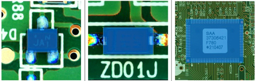
Capacitors are often categorized according to the conductor or dielectric material, which gives rise to many types, and we only consider two of them which are chip capacitors as C-CHIP and the classic capacitors with two leads as CAPACITOR. We also consider chip resistors as R-CHIP, L-CHIP to indicate an inductor chip, COIL as part of transformers, Light-emitting-diode as LED, Integrated Circuit as IC, TRANSISTOR, and DIODE as shown in Fig. 2, the samples of all 9 classes covered in this study.
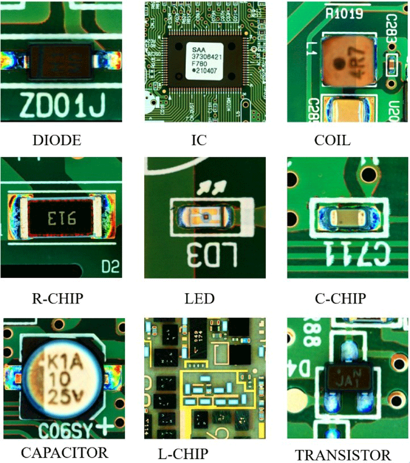
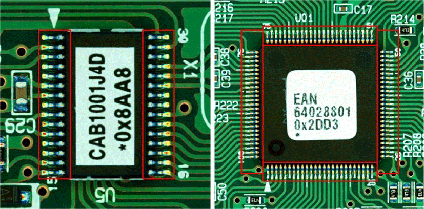
The component image used in registration and inspection is not an image of the entire PCB as shown in Fig. 2 but the image of the part to be inspected is cut out separately from the PCB image. A 700 × 700-pixel image is extracted from the entire PCB with one component to be inspected located on the center of the image. Components mounted on the PCB are mounted horizontally or vertically depending on the PCB design. In this study, the component with the least lead is rotated upward to change the shape of the component during the image processing step. The reason for using the 700 × 700 images is because the resolution is good enough to extract features and there is not a single component larger than this resolution. Using this resolution, it is easy to center the component and extract useful information from it and more practical to know where the components will be mounted on the PCB based on the completed design at the design stage.
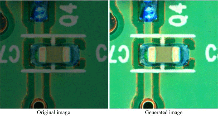
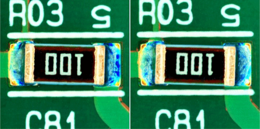
To implement a robust model for detection and classification of SMD found on PCB based on deep learning and referred to some techniques used in [20] and [21] for data sampling, variety in the dataset is more important for a suitable model for different kinds of PCB manufacturers. Therefore, image pre-processing is applied to enhance the original image so that the result is more convenient for subsequent operations and applications than the original image. There are several used methods such as image rotation, linear transformation, histogram transformation, gamma transformation, brightness and contrast adjustment. For brightness and contrast adjustment, increasing or decreasing β, which control the brightness, will add or subtract a constant value for each pixel. β may improve the image brightness, but at the same time, the contrast may be reduced. Therefore, β will be used to reduce this effect. We also need to control the value of brightness β because if we add more brightness the image may lose some details of the original bright area and cause the saturation.
Generally, to adjust the brightness and contrast, they use the multiplication and an addition with a constant as shown in the next equation.
where the parameter α>0 and β control the contrast and brightness respectively. f(x) is the input image pixel, g(x) is the output image pixel and x is a color component value R, G, and B.
In this study, the value of α depends on the initial image mean μ1 which is the image pixel intensity and the target image mean μ2.
Here β is the mean difference between the initial image and the target image.
As shown in Fig. 3, this is the representation of C-CHIP class training data distribution in grayscale based on mean and standard deviation where the data distribution is not enough because there are some missed data in the circle which can be an issue as we need to make a robust deep learning model for PCB component classification and detection.
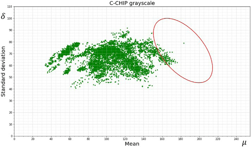
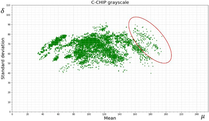
Therefore, after applying the method explained above by increasing the image brightness and contrast, we generate some new images as shown on the circle in the circle. However, the mean intensity below 30 is not useful because the image is too dark while the mean intensity above 200 is too bright with some color saturation.
The result of this illumination variation as shown in Fig. 5, the preprocessed image is brighter than the input image and the data distribution is wider than before.
As the aim of this study is focused on the classification and detection of components, collecting training data taken at different scales is more helpful for the classifier to learn the same component at different scales.
Many important ideas in geometry can be understood using transformations. As explained in the previous section, the devices are small in size (micrometer) and during the device printing, the rotation of the device to a very small angle result in uncertain camera calibration.
Here are geometric transformations consisting of rotations about the original image. Let us consider a rotation of the original image through a slight angle θ. The angle is a fixed angle between -5 to +5 degrees same as some cases in the real PCB components. Any point (x, y) in the plane rotates at a distance from the origin based on the angle θ with the positive x-axis, as illustrated in Fig. 7 below.
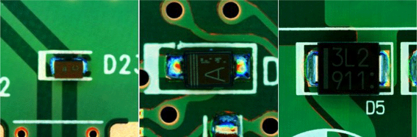
In collected data, they are some data in the same class with different shapes and sizes as shown in Fig. 8, these are all IC components, but the left component has many small leads on both two sides while the IC on right has many leads on four sides of the component. This is one of some features which differentiate the IC from other components. As we focus on the large classification to make a robust model for SMD detection, the model will learn the component in their different form and shapes.
In this paper, the method of computer vision detection is used to classify the various PCB components which are very important to train the model with an image containing information about PCB components. However, these components appear in different types according to their size and shape. The dataset used in this study is obtained from a PCB assembly company.
Component annotation is completed using a graphical image annotation tool and label object bounding boxes in images. The annotation files are stored in XML format with the image name, component location, component type.
The component location is the pixel coordinates of the target object as shown in Fig. 9 to localize the component’s bounding box, finally, the component type is the type that belongs to all 9 classes taken into consideration in this study. Each component has its characteristics that facilitate the model during the feature extraction on the backbone stage. Therefore, during the labeling, we also include the component lead as shown in Fig. 9 where DIODE has two leads, TRANSISTOR has three leads and IC has many leads.
YOLOv3 has the advantages of detection speed and accuracy and meets the real-time requirements for object detection. However, YOLOv3 has many backbone network parameters and requires high hardware performance, which is not conducive to the popularization of applications because it consumes a lot of memory as shown in the results of our experiments. On the other hand, YOLOv4 is an important improvement of YOLOv3 by the modification of the architecture in the Backbone and the Neck based on BoF (bag of freebies) and BoS (bag of specials), the Path aggregation network (PAN) [22] and the Cross-iteration batch normalization (CBN) [23]. The BoF improves the accuracy of the detector without increasing the inference time while BoS improve the accuracy of object detection. Hence, the YOLO v4 became more efficient and suitable for single GPU training and fust during inference with good accuracy.
Object detection models utilize anchor boxes to make bounding box predictions. Understanding and carefully tuning the model with customized anchor boxes can be a very important step to improve the object detection model’s performance, especially when the objects are in different shapes. The anchor’s significance is that its size predefines the target’s most likely length and width to be detected. In the data preprocessing of the YOLOv3, we usually use K-means to cluster the target sizes in the training set to generate nine most likely target anchors, each with its width and height. The size of the images in the dataset is often not uniform, and all images, whether for training or test in the YOLOv3 or YOLOv4, need to be resized to 608× 608 first. Therefore, the anchors are generated after resizing the training set image in advance. The advantage of this is that all the data are resized in advance to meet the size of the network input, and the width or length of the anchor can be directly used as the threshold of the effective receptive field size in the three anchors distribution layers. After calculation of the PCB train dataset, the sizes of the 9 anchors generated after normalizing are (39, 20); (72, 37); (125, 69); (193, 102); (234, 158); (303, 146); (381, 219); (286, 327); (457, 421).
IV. EXPERIMENT AND RESULTS
We implement YOLO v3 and v4 algorithms to classify our custom PCB dataset classified into 9 different classes include C-CHIP, R-CHIP, DIODE, TRANSISTOR, L-CHIP, CAPACITOR, IC, COIL and LED which are electronic components found on a PCB board. These algorithms had shown good performance on different state-of-the-art datasets like MS coco, Pascal VOC, and others more. The purpose is to provide a fast detection system of large classes without consideration of the component sizes. We resized all the original images from 700x700 pixels to 608x608 pixels and all experiments were performed in the environment as shown in Table 2.
| Device | Configuration |
|---|---|
| Operation System | Windows 10 |
| Memory | 32GB RAM |
| Processor | Intel Core i7-6700K CPU @4.00GHz |
| GPU accelerator | CUDA 10.2, cuDNN 8.0.2 |
| GPU | NVIDIA 2x GeForce GTX 1080 |
We trained these models with the same amount of training dataset, same test set and the same 9 anchor boxes to check which model is more suitable for SMD detection and classification. For each class in the training set, we select at least 1000 images to build a robust model for electronic components based on different sizes and shapes. Per class, 80% of the data were for training data and 20% for the validation set.
| Num | Class | Training set | Test set |
|---|---|---|---|
| 1 | C-CHIP | 8202 | 2900 |
| 2 | R-CHIP | 6909 | 1610 |
| 3 | TRANSISTOR | 3194 | 7491 |
| 4 | COIL | 1662 | 410 |
| 5 | DIODE | 3443 | 1130 |
| 6 | LED | 1401 | 1599 |
| 7 | CAPACITOR | 1028 | 1126 |
| 8 | L-CHIP | 1000 | 173 |
| 9 | IC | 3407 | 3178 |
During the inference, we tested the model with enough new data also based on different sizes and shapes to verify how good are these models in the detection and classification of PCB components. We refer to the real situation where we may find a lot of test data.
We compare the model predict class with the ground-truth class. As shown in Table 4, If the predicted class and the ground-truth class are the same, the model classifies well the component which is pass. On the other hand, if the predicted component is different from the ground-truth component, the model fails to make a good classification of the component.
The results of these two algorithms applied on SMDs are interesting because the detectors are fast, accurate with fast detection and classification average time. However, there are some problems of misclassification and detection failure for C-CHIP and R-CHIP. This is the case where the model confuses the C-CHIP component to an R-CHIP and vice-versa, also there are some components that the model could not recognize at all.
In YOLOv4, the use of BoF and BoS make the object detector accurate by increasing the training cost but by improving the inference cost.
To verify the importance of applying the data augmentation proposed in this research, we add an experiment with original data without applying the data augmentation on YOLOv4 as shown in Table 4. The experiment with data augmentation shows good results compared to the experiment on original data without data augmentation.
Table 5 shows the model evaluation where it achieves an mAP of 99.23% by using an intercession-over-union (IoU) threshold of 50% and an mAP of 99.16% for a threshold of 75%.
| Model | mAP50 | mAP75 | Precision | Recall | F1-score |
|---|---|---|---|---|---|
| YOLOv4 | 99.23% | 99.16% | 0.84 | 0.99 | 0.91 |
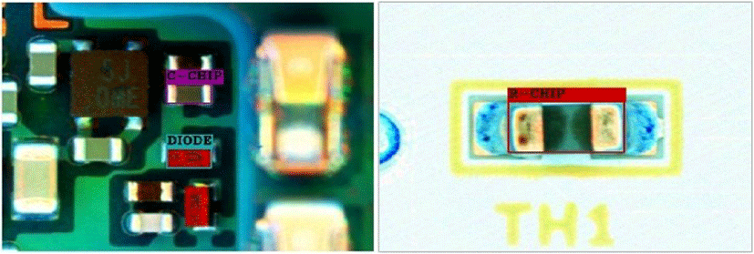
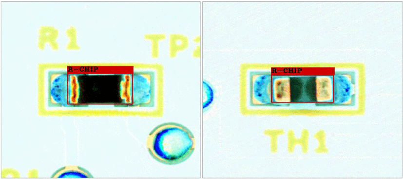
Fig. 11 shows the two fail components in the YOLOv4 experiment result. Our prediction is to detect the component located in the center of the image. But the image on left, the detector detects two devices which are C-CHIP and Diode, and both are close to the center of the image, but none is in the center and the Diode probability is higher than C-CHIP. On the other hand, the image on right detects the component as an R-CHIP while it is a C-CHIP. However as shown in Fig. 12, this C-CHIP has some similarities with R-CHIP like the black part inside the component which is one of the main features of the C-CHIP device.
V. CONCLUSION
In this paper, to classify and detect SMD on the PCB board, the characteristics of each component are considered, the boundary box of the components is generated based on our target object, and classes are defined. And most important we used some data preprocessing and augmentation methods to build a robust model which detects and classifies the SMDs during the inspection step. As we used our customized data, the anchor boxes were also modified. To build a robust deep learning model we used the large classification so that each class will have various data shapes and sizes. We customized the YOLO algorithms based on our dataset of electronic SMDs for detection and classification tasks. The effectiveness and robustness of these models are shown in the previous section. But based on results, YOLOv4 always shows the best results compared to the other models. YOLOv4 detector is very accurate and effective for SMD detection and classification with an mAP of 99.16% for a threshold of 75%. However, there are still errors or misclassified and undetected data in our models like some components that failed to be classified and detected.
Based on these limitations in this study, we will extend our analysis by collecting more data with depth information and making a small classification taking into account the size and shapes of the device.