


I. INTRODUCTION
PLLs consist of a phase/frequency detector (PFD), a charge pump (CP), a loop filter (LF) and a voltage controlled oscillator (VCO), whose output is fed back to the PFD. The PFD compares an external reference signal and the VCO output signal and produces two digital signals (Up and Down), with the width of these two signals being determined by their frequency and phase. The CP converts the PFD output signal into a current that is fed into the LF, which determines the output LF voltage. The LF output voltage causes the VCO to generate a single frequency signal. Voltage fluctuation in the LF output causes a proportional variation in VCO output signal. The LF output voltage fluctuates when the PLL is in-lock status; this causes the VCO output signal to have a large amount of phase noise with spur [1].
Various PLL architectures are proposed for low phase noise performance. In general, PLL prefers narrow loop bandwidth for low phase noise [2], [3]. However, it can’t suppress the out of stop frequency phase noise from VCO and is not suitable for some application. Low VCO gain design is a widely used method for low phase noise [4]. It consists of a dual loop and switched-capacitor networks for wide output frequency selection with drawback of long locking time. Linearization techniques and high order loop filter are used to reduce phase noise by avoiding non-linearity such as dead-zone and current mismatch originates from PFD and CP [5]. But, there is a trade-off between the non-linearity from the CP and noise contribution during “on-time”. Another way to reduce phase noise is to use active loop filter and two ring voltage controlled oscillators [6], [7]. Therefore, it requires LDD-regulator which needs a high DC supply voltage.
In this brief, we propose a novel PLL architecture with the current compensating scheme, and a novel VCO consisting of voltage controlled resistor (VCR) and latch type delay cells. The PLL decreases phase noise by using two CPs, MCP and SCP. The SCP provides its current to LF in the opposite direction of UP/DN MCP current. It reduces the current flowing through LF. The voltage fluctuation of LF in the proposed PLL is smaller than that of conventional PLL at the same magnitude of LF flowing current. In this way, a low phase characteristic can be obtained with the current compensating scheme.
II. PROPOSED PLL ARCHITECTURE
The output voltage of LF in-lock status fluctuates and its magnitude depends on the transfer function of PLL. Even though PLL is in-lock, there is a slight difference in the magnitude of charging and discharging current. Consequently, it causes the random voltage fluctuation. This random voltage fluctuation of LF creates a lot of spurs that deteriorate the phase noise characteristic of PLL. Therefore, the phase noise characteristic can be improved if the magnitude of voltage fluctuation can be decreased. In order to improve the phase noise characteristic, we propose the current compensating scheme by using two CPs as shown Fig. 1.
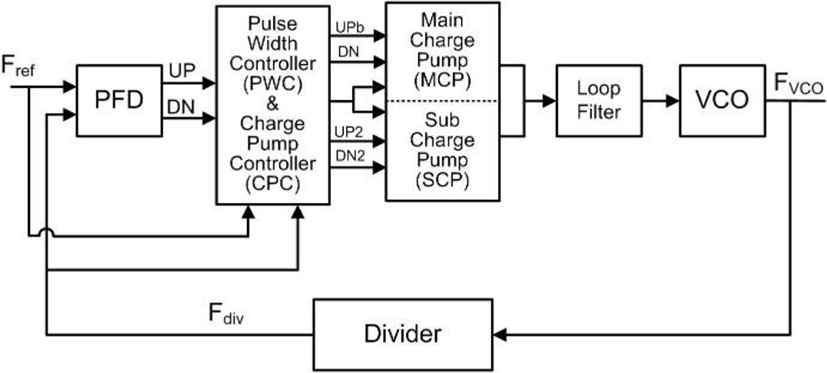
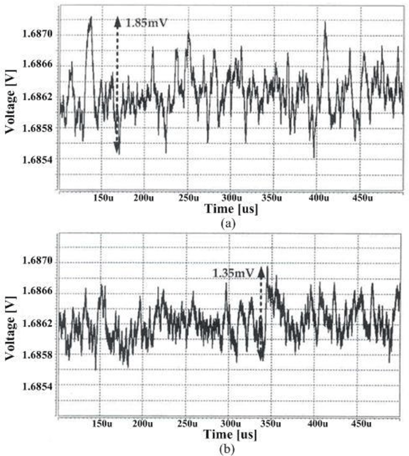
Figure 2 shows the concept of the proposed PLL with two CPs. The architecture uses two CPs with UPb/DN for MCP and 180° phase shifted UP2/DN2 for SCP. When MCP current causes the LF voltage to fluctuate, SCP current compensates the LF voltage fluctuation. While PLL is in-lock, MCP provides UPb/DN current to LF and it makes LF output voltage rise/fall. Simultaneously, the SCP reduces the current flowing through LF and it makes LF output voltage rise/fall slowly. This kind of current compensating scheme minimizes the LF output voltage fluctuation and improves the low phase noise performance. The simulation results are shown in Fig. 3. Conventional PLL with 30 μA of CP current and the proposed PLL with 60 μA of MCP current and 30 μA of SCP current have the maximum voltage fluctuation of 1.85 mV and 1.35 mV, respectively. The proposed PLL results in 0.5mV reduction in maximum LF output voltage and less deviated waveforms from the average LF voltage.
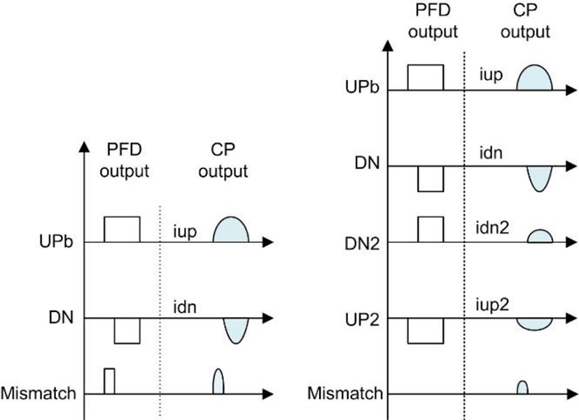
The timing mismatch in signals for MCP and SCP is kept very small, almost none because it can cause additional phase noise and spurs. PFD generates two different synchronized signals, UPb/DN for MCP and 180° phase shifted UP2/DN2 for SCP.
The size of PMOS transistors is larger than that of NMOS transistors in CP and it can cause also timing mismatch. By adding additional dummy transistor to the NMOS transistor, the input capacitance of PMOS and NMOS transistors are made equal. It makes the rising and falling time of PMOS and NMOS transistors same.
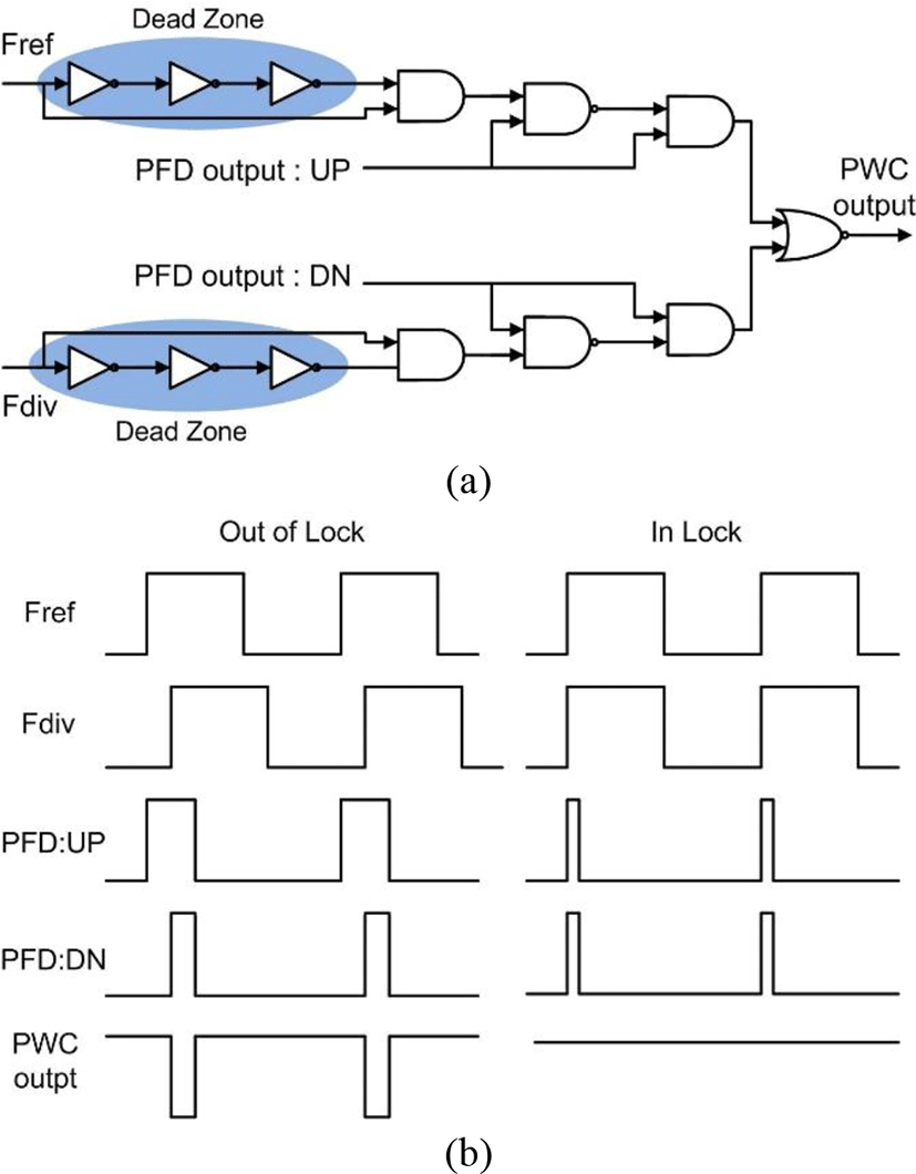
Here, we use an adaptive bandwidth concept for fast locking and low phase noise. An indicator for PLL locking status is required to adaptively control the loop bandwidth. Pulse width controller (PWC) generates locking status indication signal. The PWC uses a dead zone characteristic of PFD. The PWC is designed for PFD to generate no output signal in case when the PLL is near in-lock [8]. Fig. 4 shows the circuit and signals of PWC.
Its output signals control the charge pump controller (CPC) output voltage to generate the relevant magnitude of MCP current according to the locking status. The PWC output signals are fed into the SW controller which generate SW/SWb signals to control SW1/SW2 transmission gates as shown in Fig. 5. When the PLL is out-of-lock, SW1 is on and SW2 is off. When the PLL is near in-lock, SW2 is on and SW1 is off. CPC provides two different voltages of Vcon1 for MCP depending on the PLL locking status and a single voltage of Vcon2 for SCP.
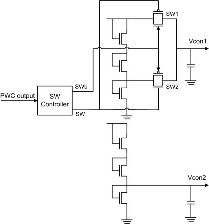
When the PLL is out-of-lock, MCP current is 400 μA using PWC and CPC. These make the PLL have wide bandwidth for fast locking. When the PLL is in-lock, MCP current reduces to 60 μA. It makes the PLL have narrow bandwidth for low phase noise. The current magnitude of SCP is always 30 μA regardless of locking status.
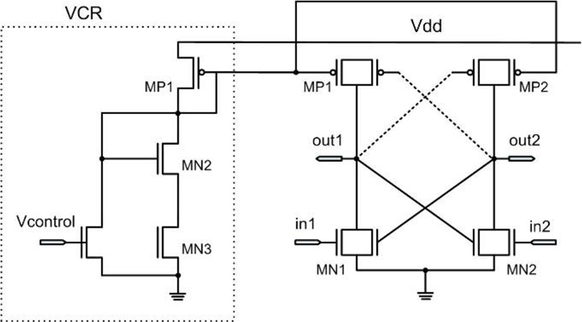
Ring oscillators have the advantage of wider oscillation frequency range and a smaller die size but poor phase noise characteristics compared to high-Q LC oscillators. In this brief, we propose a novel VCO by using a VCR, which linearly converts voltage into current, and the three-stage ring oscillator with latch type delay cells. The latch type delay cell has short active on-time of transistors and it improves phase noise characteristic. The proposed VCO architecture with VCR is shown in Fig. 6. VCR generates a linear current proportional to input voltage and the latch type VCO generates a constant frequency corresponding to this current. The proposed VCO has a 260 MHz/V gain and very linear oscillation frequency range from 810 MHz to 1.4 GHz.
III. EXPERIMENTAL RESULTS
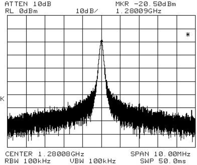
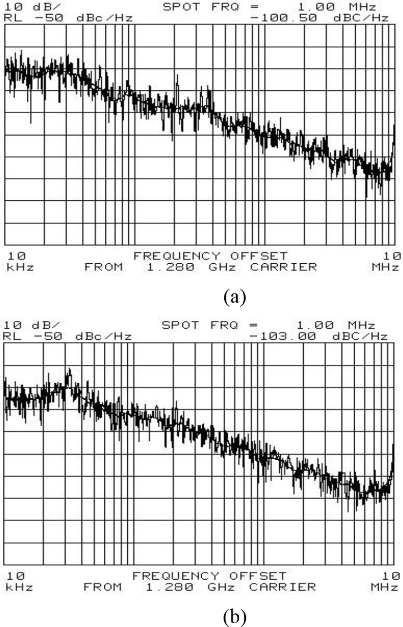
The proposed PLL with two CPs and conventional PLL with one CP have been fabricated in 0.35 μm CMOS process. The measured output spectrum of the proposed PLL is shown in Fig. 7. The measured phase noise of conventional PLL and the proposed PLL at 1 MHz offset from 1.28 GHz carrier frequency are shown in Fig. 8. Conventional PLL shows phase noise of −100 dBc/Hz and the proposed PLL shows around −103 dBc/Hz at 1 MHz offset, respectively. It demonstrates that the proposed current compensating scheme results in 3 dBc/Hz phase noise improvement compared to the conventional PLL with one CP. The improvement is not as much as impressive compared to the simulation result that showed the 0.5mV reduction from the 1.85 mV to 1.35 mV as shown in Fig. 3. The measured results are summarized in Table I.
| Technology | CMOS 0.35 |
| VDD | 3.3 V |
| Output Frequency | 810~1400 MHz |
| Reference Frequency | 20 MHz |
| Phase Noise | −103 dBc/Hz @1 MHz |
| Die Area | 700 μm × 450 μm |
IV. CONCLUSION
In this brief, we proposed a novel PLL architecture with the current compensating scheme to improve phase noise performance. The SCP provides its current to LF in the opposite direction of MCP current. It reduces the current flowing through LF. The magnitude of voltage fluctuation on LF in the proposed PLL is smaller than that of conventional PLL at the same magnitude of LF flowing current. In this way, a low phase characteristic can be obtained with the current compensating scheme. The PLL with the current compensating scheme has been fabricated in a 0.35 μm CMOS process. The measured results show that the proposed PLL results in the phase noise improvement of 3 dBc/Hz at 1 MHz offset compared to the conventional PLL.